Monolithic Optoelectronic Transducer
The optical microchips are fabricated entirely by employing standard silicon processing, such as ion implantation, Chemical vapor deposition of silicon dioxide insulationg and silicon nitride waveguide films, and anisotropic reactive ion etching. The combination of anisotropic reactive ion etching and thick chemical oxide depositions create the smooth quantrant like spacers at either end of the optical link. These spacers provide for the smooth bending of the optical waveguide required to minimize bending losses. For the most part of the optical length light travels horizontally, while at the emitter and detector ends it goes vertically. The high coupling emitter-detector external efficiency (over 40%) is due to the self aligned emitter light emitting junction lying just underneath the up-going segment of the silicon nitride waveguide. The devices are completed with the deposition and patterning of the cladding layer, metal interconnects and open microfluidic channels.
Monolithic Optocoupler.
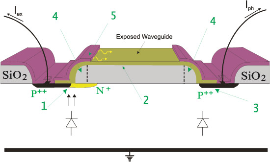
Schematic of the monolithic optocoupler featuring the avalanche LED (1) the silicon nitride waveguide (2), the p/n junction detector (3), the silicon dioxide spacers (4) and the cladding layer (5).
Each optocoupler has it own emitter, its own self aligned waveguide while the detector is common and shared by all optocouplers on the chip. The selection of the optocoupler is made possible by multiplexing the emitter bias. This common detector scheme greatly simplifies the readout electronics and provides the same detection characteristics for all optocouplers.
Fabricated Device.
 |
 |
View of the optocouplers from the emitter side (left) and the single detector side (right). The waveguides are 150 nm thick, 8 um wide, have a length 2400 um, are shown as pink strips originating from the emitters (left) and are converging to the common detector shown on the right.
The open microfluidic channels are integrated on wafer scale. They are created after SU-8 film is deposited and patterned on the processed chips. A cover layer on top with two opening for the inlet and the outlet port completes the channels. Such cover layer is made by an elastomer to provide sealing and is part of the device packaging.
Single optocoupler array chip.

Photograph of an optocoupler chip showing the single sided contact geometry and the SU-8 Microchannels meandering over the nine different optocouplers. The emitters are shown on the left and the common detector on the right. Τhe single sided contact pad geometry allows for state of the art direct contacting eliminating the need for wire and die bonding.