Si nanowires and nanodots and their applications
The activity on semiconductor nanostructures started within this research group at the early nineties. It has been conducted within different EU projects, and worldwide pioneering results include the following: Development of a fabrication technique of light emitting silicon nanowires using the top-down approach (1985), development of light emitting devices based on Si nanowires (1998), development of the growth and investigation of the properties of single and multiple two-dimensional arrays of Si nanocrystals (NCs) with controllable size, embedded in SiO2 and development of Si NC memories.
Currently, the group focuses on the following activities:
Two-dimensional arrays of Si nanocrystals embedded in SiO2 for solar cell applications: Investigation of their electrical and optical properties
SiNWs by metal-assisted chemical etching: synthesis, characterization and applications
Porous Si membranes
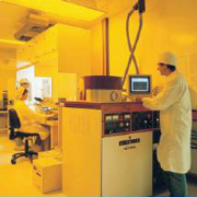
The group has important expertise and know-how, as well as different proprietary processes in the field of porous Si membranes. Existing processes include the fabrication of thick porous Si membranes locally on the Si substrate, porous Si free standing close-type membranes over cavity fabricated in a single electrochemical process and porous Si cantilevers and suspended membranes fabricated by electrochemistry. The porous material is composed of either randomly distributed pores or straight vertical pores. Applications developed within the group include thermal sensors, nanocooling devices and RF passive devices integrated on Si. Porous Si membranes are used as substrate for thermal or RF isolation from the Si substrate.
Porous anodic alumina on Si
Porous anodic alumina thin films on Si with highly ordered hexagonally arranged pores are fabricated by electrochemistry and used either as template for growing nanowires and other nanostructures within the pores or as masking material for Si nanopatterning. Porous anodic alumina is also used as a high-k dielectric material in memory devices and in metal-oxide-metal (MIM) capacitors.
High performance on-chip RF passives and memory devices using novel materials and technologies
Key results in 2010 within this activity are as follows:
High performance RF and mm-wave transmission lines were fabricated on porous Si membranes. Porous Si provides excellent shielding to the lossy Si substrate. It is thus possible to fabricate on-chip passive devices on the Si wafer that show similar comparable characteristics with the best off-chip corresponding devices. Co-planar waveguides were fabricated and tested at frequencies up to 110GHz.
Novel high performance MIM capacitors using porous alumina dielectric and exhibiting large capacitance density and low leakage current were also demonstrated.
Charge trapping memory devices using porous anodic alumina dielectric on a thin anodic SiO2 layer, both fabricated in a single electrochemical step, were also demonstrated and their charging properties investigated.
Metal-insulator semiconductor (MIS) capacitors using silicon oxinitride (SiON) dielectric were also investigated by electrical measurements.