


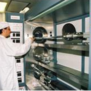
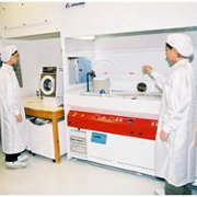
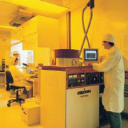
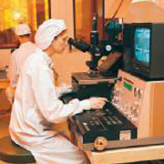


| a. Lateral electrical transport, optical properties and photocurrent measurements of 2D arrays of Si NCs embedded in SiO2 We investigated the lateral electronic transport, optical and photo-electric properties of two-dimensional (2D) arrays of oxidized silicon nanocrystals (Si NCs) of different sizes grown on quartz by low pressure chemical vapor deposition (LPCVD) and subsequent thermal oxidation. The films contained Si NCs with controlled sizes ranging from less than 2 nm up to 12 nm. The Si NCs within the films were separated with grain boundaries or silicon dioxide tunnel barriers. The electrical measurements showed that current in the films is mainly determined at low temperatures by tunneling, whereas at high temperatures by thermionic emission over the barriers. Charge traps at the interfaces of the Si NCs with the oxide or the grain boundaries caused considerable hysteresis in the current-voltage characteristics. Hydrogen passivation of the charge traps reduced the hysteresis effect and the activation energy of the thermionic emission, whereas the current-voltage characteristic after hydrogen passivation showed a superlinear shape, resulting from the collective effect of the Si NCs involved in the transport which were separated by tunnel barriers and had Coulomb gaps due to their small sizes. Activation energy corresponding to tunneling through the oxide tunnel barriers between the Si NCs was correlated with the charging energy of the Si NCs within the layers, i.e., the energy needed by the carriers to overcome the Coulomb gaps of the Si NCs in the current path. Absorption measurements showed a clear increase of Si NC energy bandgap with decreasing NC size due to quantum confinement. Also, higher absorption than bulk Si was observed in the visible and ultraviolet regions. Photocurrent and absorption spectra showed similar dependency on energy, confirming that photocurrent was due to carriers generated in the Si NCs within the films, when energy of illumination became higher than the energy bandgap of the Si NCs. Light emission at room temperature was observed only in the film containing Si NCs smaller than 3nm. This film showed no measurable photocurrent. This effect was due to the strong localization of the photo-generated carriers within the Si NCs of these sizes which favored radiative recombination of the carriers and excluded photocurrent. b. Si nanowires by metal-assisted chemical etching Si nanowires (SiNWs) are synthesized by the single-step metal-assisted chemical etching (MACE) technique in AgNO3/HF aqueous chemical solution. The obtained SiNWs are of high crystalline quality, since they result from etching of the crystalline Si skeleton. The nanowire length is monitored by changing the immersion time of samples in the solution. SiNWs with length ranging from few μm up to several tens of μm can be obtained. We investigated in detail the growth rate of NWs as a function of temperature (in the range of 20-50οC) and found that it increases monotonically with temperature. An example of cross sectional scanning electron microscopy (SEM) images at three different temperatures are given n fig. b1. In fig. b2 we see a top view of the sample surface, which reveals that long SiNWs form bundles, attracted by capillary forces. We also investigated the surface morphology of the SiNWs and found that it depends on their length. Short NWs are very smooth, while longer ones show a nanoporosity all along their surface. This work was presented in Fourth International Conference on Micro-electronics, Nanotechnologies and MEMs which took place in Athens on 12-15 December 2010. c. Photoluminescence–induced oscillations in porous anodic aluminum oxide grown on Si. A method to estimate porosity Porous anodic alumina (PAA) films grown directly on Si substrates show oscillations in their photoluminescence (PL) spectra. These oscillations are ascribed to PL-induced interferences within the Farby-Pérot optical cavity formed by the PAA film on Si, that involve the air/oxide and oxide/Si interfaces. The existence of the PL oscillations is indicative of the high quality of the interface of the PAA film with Si, which is both planar and smooth. Using these PL-induced oscillations we can develop a sensitive optical method of measuring the porosity of the PAA film if the film thickness is known. This method is based on the calculations of the effective refractive index of the PAA film derived from the PL-induced oscillations. This value of the estimated refractive index is introduced into the Bruggeman equation to derive the film porosity. References: d. Si microplate technology for on-chip local RF isolation Co-planar wave (CPW) transmission lines were fabricated on porous Si microplates electrochemically developed on low loss substrates. The substrates used were p+ Si wafers of resistivity 0.001-0.005 Ωcm. The thickness of the porous Si microplate was 150 µm. The CPW lines were designed to have 2 different values of characteristic impedance, namely 50 and 145 Ω. The lines were characterized up to 40 GHz. De-embedding techniques were used to extract the values of the characteristic impedance, the quality factor and the attenuation constant. It was shown that attenuation lower than 0.3 dB/mm can be achieved at 40 GHz for both values of the characteristic impedance used. This value is several times better than commonly quoted values in the literature. Also a quality factor of 20 was demonstrated at 40 GHz. The experimental results were reproduced using simulations with the HFSS program. The CPW lines were then tested up to a frequency of 110 GHz also producing results that are better than the state-of-the-art performance of on-chip mm-wave passives. e. Fabrication and characterization of high performance anodic alumina MIM capacitors We fabricated and characterized Metal-Insulator-Metal (MIM) capacitors using as dielectric a thin porous anodic alumina (Al2O3) layer between two Al films. The Al2O3/Al stack was grown electrochemically by partly anodizing an Al film on Si, while a top Al film was then deposited on the aluminum oxide and patterned in order to define the capacitor area. The obtained MIM capacitors exhibit at the same time large capacitance density (above ~5 fF/µm2), low leakage current density (below ~10-9A/cm2 at 2V) and good thermal stability of operation, demonstrated by an α coefficient that changes by less than 10% for temperature changes of the order of 100K. The temperature stability was further demonstrated by the low leakage current density (below ~7x10⁻⁹A/cm2) even at temperatures as high as 420K. These characteristics satisfy the ITRS requirements for MIM capacitors in the next years. Additional advantages of the demonstrated capacitors is the simplicity of fabrication, that reduces the cost, and the fact that the entire fabrication is CMOS compatible and room temperature which is very important since MIM capacitors are back-end devices.
Ref. E. Hourdakis and A.G. Nassiopoulou, IEEE Transactions on Electron Devices 57 (10), art. no. 5535075, pp. 2679-2683 (2010) Using the same fabrication scheme as described above we fabricated and characterized MIM capacitors using barrier-type anodic alumina (Al2O3) as the dielectric instead of the porous anodic alumina previously used. The obtained capacitors exhibited large capacitance density (above 7 fF/µm2) and very small leakage current for a voltage range between -2 V and 2 V (below the background noise of our measurement system). It was shown that there is a significant improvement in both the value of the capacitance density and the value of the non-linearity coefficient α compared to the porous alumina capacitors. Ref. E. Hourdakis and A.G. Nassiopoulou, Microelectronics Engineering, in press (submitted in 2010) f. Fabrication and characterization of charge trapping MOS memory structure using anodic alumina dielectric A novel charge-trapping-type MOS memory structure using a high-k dielectric on a thin SiO2 layer, both fabricated in a single electrochemical step, was demonstrated. The high-k dielectric was a porous anodic aluminum oxide layer (Al2O3, PAA) that played the combined role of the charging medium and the control oxide. The tunnel oxide was an electrochemical SiO2 layer grown through the pores of the anodic alumina layer. It was demonstrated that this simple MOS structure shows comparable memory characteristics (charging/discharging, memory window and retention) with those of charge trapping type memories using high-k dielectrics in a complicated gate dielectric stack, fabricated using expensive equipment. It could be a solution towards a novel low cost charge trapping dielectric layer for memory devices. Ref. E. Hourdakis and A.G. Nassiopoulou, Microelectronics Engineering, in press (submitted in 2010) g. Electrical properties of ultra thin SiON films We combined electrical and structural characterization with analytical and spectroscopic measurements in order to fully analyze oxynitride nanofilms that were produced in a mini batch type plasma nitridation reactor. We demonstrated that for the investigated samples the result of nitridation is different in the 2 nm thick SiO2 films compared to the 5 nm thick films. In the first case, nitridation results in an increase in the initial film thickness with a consequent decrease in leakage current and an increase in equivalent oxide thickness (EOT), while in contrast, nitridation of the 5 nm thick SiO2 films leads to a reduction of both the leakage current and EOT. Finally, we demonstrated that the applied nitridation process results in the desired nitrogen profile with high nitrogen concentration near the top surface or the middle of the SiON film and low nitrogen concentration near the SiON/Si interface, that leads to a relatively low density of interface states (~1011 states/cm2) for non-annealed films. * Ref. E. Hourdakis, A. G. Nassiopoulou, A. Parisini, M. A. Reading, J. A. van den Berg, L. Sygellou, S. Ladas, P. Petrik, A. Nutsch, M. Wolf, and G. Roeder, J. Vac. Sci. Technol. B 29, 022201 (2011) (accepted in 2010, published in 2011) Plasmonic metamaterials In the last years, increasing amount of attention has been directed toward the assembly of metal nanoparticle building blocks into ordered structures for diverse applications that include, among others, (bio)sensing and optoelectronic devices. In some cases structure determines the material properties, and the term metamaterial is used. Unlike metamaterials based on metallic nanorods, split-ring resonators, or cut-wire pairs, which operate at a specific polarization mode of the electromagnetic (EM) field, metal–dielectric-metal nanosandwiches, due to their cylindrical symmetry, offer the possibility for designing polarization-insensitive metamaterials. Moreover the problem of assigning effective EM parameters to a heterogeneous medium is an important issue and various homogenization methods have been proposed. Usually one imposes the scattered wave from a planar slab of the heterogeneous medium in the far-field zone, to be the same with that scattered from a slab of a hypothetical homogeneous material. But this technique often leads to nonphysical material parameters as a result of forcing a homogeneous material to reproduce exactly the features of the wave field scattered by the actual heterogeneous medium. We used a homogenization method based on systematic full-electrodynamic complex-band-structure calculations, and deduce the effective permittivity tensor of a uniaxial photonic crystal consisting of consecutive hexagonal arrays of aligned metallic nanorods of finite length. The form of the obtained permittivity tensor over a relatively broad low-frequency region, where homogenization is applicable, suggests the occurrence of unconventional refractive behavior, namely, negative refraction and self-collimation. Moreover, in the frequency region where negative refraction occurs, a finite slab of the crystal possesses eigenmodes that form flat bands outside the light cone. These eigenmodes allow for transfer of the evanescent components of an incident wave field to the other side of the slab, thus enabling subwavelength imaging. Schematic view of a layered metal/silica/ metal nanosadwich metamaterial. Arrays of metallic nanorods can be used for negative refraction and subwavength imaging. Dual photonic-phononic spectral gap materials Photonic crystals with submicron periodicity have band gaps in the visible and near infrared part of the spectrum promising applications in optical sensors and telecommunications. Phononic crystals on the other hand are mainly studied in more macroscopic length scales in the order of millimeter. Only very recently, elastic composites with submicron periodicity were demonstrated with acoustic band gaps in the gigahertz range. Tailoring both acoustic and optical properties on the same system can lead to applications which require better control of the acousto-optic interaction. Phoxonic crystals having dual spectral gaps for both photons and phonons could lead to promising applications. We have studied 3D metallodielectric crystals, 2D perforated Si slabs and Si pillars on a silica slab but also 1D multilayer structures, and predicted simultaneous band gaps for both light and sound at different frequencies in all geometries. Moreover by analyzing the acousto-optic interaction in 1D multilayers we demonstrate that the simultaneous light and sound localization in a phoXonic cavity leads to enhanced acousto-optic interaction and multiphonon emission-absorption processes. |
|
Results
|