|
LABORATORIES
AND CENTRAL FABRICATION FACILITIES AT IMEL
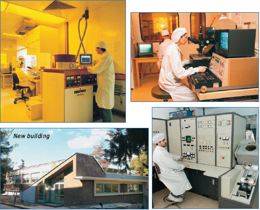
The facilities
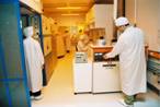
and equipment of IMEL include a full silicon processing
laboratory in a clean room, equipped with
lithography (optical, e- beam) and etching tools, thermal
and chemical processing facilities, ion implantation,
deposition of metals, dielectrics and poly- nanocrystalline
silicon by physical and chemical processes (LPCVD, sputtering,
e-gun and thermal evaporation), and process inspection
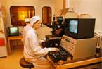
equipment. Satellite laboratories include electrical
and optical characterization, micromachining and packaging
laboratory, resist development laboratory, electron
microscopy (SEM, STM/AFM), sensor characterization and
testing equipment.
The clean room area for thermal, chemical and reactive
ion etching processes of the Institute has been fully
upgraded to class 1000, while lithography area to class
100, in the year 2002.
A new building of the Institute has been constructed
in 2006 to host the electrical, optical and structural
characterization laboratories. A photograph of the building
in the final stage of construction is shown in the figure
below.
NANOTECHNOLOGY AND MEMS LABORATORY. ACCESS PROVIDED
The laboratory is certified under ISO 9001:2000 (Si processing and electrical characterizartion) and under ISO 17025:2005 (electrical measurements).
The equipment available and the expertise and competences include the following:
PROCESSING
Equipment |
Techniques/competences |
Silicon processing laboratory in a clean room area of 500 m2, equipped with the following:
- 4 laminar flow chemical benches
- 7 horizontal hot-wall furnace tubes
- 2 horizontal LPCVD tubes for
nitride, oxide (TEOS), polysilicon
- 1 horizontal LPCVD tube for LTO
- Ion Implanter (EATON medium
current, 200 KeV)
- Optical lithography systems (resolution down to 0,6 μm)
- reactive ion Etcher
- Metallization equipment (thermal, e-gun evaporation, sputtering)
- Process inspection equipment
Processing equipment not in clean room:
- High Density Plasma Etcher
- Different thin film deposition systems (Sputtering, MOCVD)
|
- Nanopatterning technologies
- Plasma etching
- Growth of metals and dielectrics
- Growth of polycrystalline and nanocrystalline Si
- Growth of Si nanostructures embedded in a dielectric matrix, ordering of nanostructures
- Fabrication of MOS capacitors and MOSFETs
- Nanocrystal non-volatile memories
- Micromachining, sensor fabrication, microfluidics
- Molecular materials and devices
- Thin film devices
|
CHARACTERIZATION & MODELLING
Equipment |
Techniques/competences |
Electrical
- Several probe stations
- HP measuring systems (4142B, 4084B, 8110A, 700i series, 4140B, 4284, 4192A, 34401, 16500A)
- Keithley measuring equipment (230, 220, 617, 195A,517A)
- Oxford optistat cryostat for temperatures in the range 4.220K
- Wafer level cryogenic measurements (Janis probe station)
- Cascade Microtech Summit 9101 Analytical Probe Station for 150mm wafers
- Anritsu 37269D Vector Network Analyzer 40MHz-40GHz
Optical
- Jobin Yvon spectrometer, wavelengths 300 - 1600nm
- Ar+ laser
- HeCd 325 nm laser
- UV lamp with monochromator
- Oxford optistat cryostat, 4.2-320K
- FTIR: Bruker, Tensor 27
Morphology, structural characterization
Testing equipment
- Systems for testing of gas flow, gas pressure, acceleration, humidity sensors, biosensors and systems, microfluidics testing etc.
Modeling and simulation software
- SILVACO tools for process and device modeling (Athina and Atlas)
- Suprem and Pisces
- Floops and Floods
- Synopsis – Coventorware
- MATLAB-FEMlab
- Mentor graphics
|
Characterization of Dielectrics
- Admittance measurements (1Hz up to 1MHz, 25-150°C)
- I-V measurements (2 up to 4-terminal devices, 25-150°C)
- Charge-to-breakdown measurements
- Bias-Temperature-Stress measurements
Characterization of MIS Devices
- Admittance measurements (1Hz up to 1MHz, 25-150°C)
- I-V measurements (2 up to 4-terminal devices, 25-150°C)
- Hot-carrier stress measurements
- Bias-Temperature-Stress measurements
EEPROM device characterization and reliability measurements
Characterization of RF components
Optical characterization
- Absorption measurements, wavelength range UV-VIS-IR
- Photoluminescence (PL)
- Laser excitation: 325 nm, 457.8nm, 488nm, 514.5nm
- Spectrometer: 350nm-1600nm
- Electroluminescence (EL): 350nm-1600nm
- Photocurrent-photovoltage (UV-VIS)
- FTIR
Characterterization of sensors
- Gas sensors
- Microflow sensors
- Accelerometers
- Optical devices
- Biosensors
- Microfluidics
Modeling and simulation
- Process and device modeling
- RF modeling
|
|