NANOTECHNOLOGY AND MEMS LABORATORY. ACCESS PROVIDED
This webpage describes the clean room infrastructure of the Nanotechnology & Microsystems Laboratory, which is operated and managed by the Department of Microelectronics. Our aim is to encourage academia and industry researchers at a national and international level to get access to this infrastructure either through specific assignments or through research collaborations.
The Department of Microelectronics (former Institute of Microelectronics – IMEL) is one of the three departments of the Institute of Advanced Materials, Physicochemical Processes, Microsystems and Nanotechnology (IAMPPMN) of NCSR “DEMOKRITOS” that resulted from the merging in 2012 of IMEL with the former Institute of Advanced Materials and the Institute of Physical Chemistry.
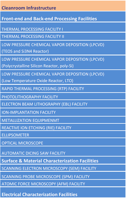
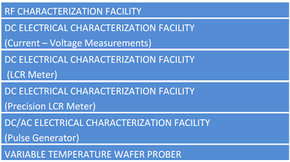
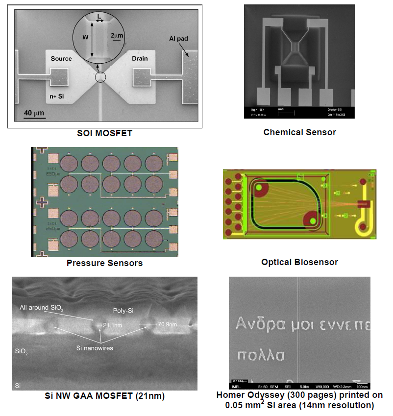
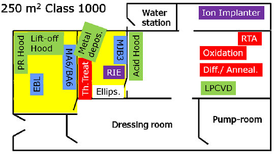
Since 2007 the N&M laboratory is certified under ISO 9001:2000 for the Si processing and electrical characterization and under ISO 17025:2005 for the electrical measurements. It comprises the cleanroom, surface and materials characterization as well as electrical characterization facilities. The cleanroom facilities include a full Si processing laboratory in a clean room area (500m2, ISO 6 and ISO 5 clean areas), equipped with unique at national level and state-of-the-art tools such as ion implanter and e-beam lithography (EBL). The newly installed 100keV modern EBL tool is capable of sub-10nm patterning on up to 150mm wafer-size.
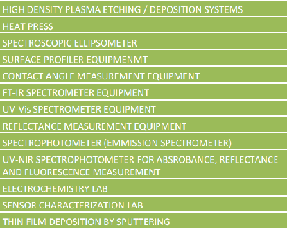
Satellite laboratories in gray-area (cleanroom environment ISO 8) include electrical and optical characterization, micromachining and packaging laboratory, chemistry laboratory for the development of resist and polymers for organic electronics, microscopy laboratories for surface and material analyses (SEM, STM/AFM), electrochemistry laboratory, sensor characterization and testing equipment and optical laboratory.
Through the years the Department of Microelectronics had developed expertise and has the knowhow to provide services in a wide spectrum of microelectronics and nanotechnology-related processes. This has been successfully proved through the successful participation of N&M lab in the I3 FP6-project ANNA, providing transnational access to research/university laboratories and SMEs.
At present, access to the Laboratory is possible either for specific assignments or through research collaborations. The scientific and technical staff of the department supports the users in all stages of the assignment. For accessing the infrastructure please send your enquiry by e-mail to services@imel.demokritos.gr.
Nanotechnology and Microsystems Labaratory Cleanroom Area
CLEANROOM INFRASTRUCTURE
Click here to download the facilities booklet
|