IMEL at a glance
Research at IMEL is carried out at EU level through its participation in European research projects, networks of excellence, and technology platforms. EU projects are across a number of specific priorities of the EU Research Framework Programme, including mainly Information Society Technologies (IST), Nanotechnology, Materials and Production Processes (NMP), Energy and Health. IMEL’s success in the above peer reviewed R&D funded programmes represents one of the strongest endorsements of IMEL’s R&D competence and reflects the world-class standing of the Institute.
On national level the expertise and infrastructure of IMEL are unique in Greece, which makes its role for the country also unique in an effort to develop novel technologies, to transfer technology and know-how to the industry and to develop human potential, which constitutes the principal driving force for an industrial activity in high technology. Furthermore, IMEL developed mechanisms to promote the field at national level through the establishment and coordination of thematic networks and scientific societies (MMN Network, Micro & Nano scientific society).
• Main Objectives of IMEL
The main objectives of IMEL are as follows:
• Long-term research into understanding phenomena, mastering processes and developing research tools.
• Development of fundamental knowledge
• Development of novel high added-value technology products and production processes
• Development of human potential by education and training activities
• Services in advanced technology
• Transfer of technology and know-howThe objectives of IMEL are in line with the government policy to promote excellence in research, high technology development and innovation at Research Institutes and to promote collaboration between academia and industry.
The objectives of IMEL are also in line with the European policy to maintain and increase EU competitiveness and sustainable development through design, development and dissemination of advanced technologies, including micro and nanotechnologies and systems. They are also in line with the EU objective to “achieve a critical mass of capacities needed to develop and exploit leading edge technologies for the knowledge- and intelligence-based products, services and manufacturing processes of the years to come”.
Due to the existing infrastructure available at IMEL for silicon processing and micro- nanofabrication and the existing expertise and know-how developed, the role of the Institute is significant in contributing to increase the technological level of the country and to spread the knowledge through collaboration with Academia in research and education activities.
• Research orientation
IMEL is mainly devoted to silicon technologies and their diverse applications in information processing, storage, transmission systems and telecommunications, environmental systems, medicine, healthcare, food industry etc.
Research Activities at IMEL are structured in 3 programmes, each of them being composed of smaller projects. A scientist is in charge of each research project, while a program representative is assigned for the management of each programme. The 3 programmes and the corresponding projects are as follows:
A. MICRO and NANOFABRICATION
• Materials for Lithography and Organic/Hybrid Electronics
• Plasma Enabled Nanofabrication: Processing, Simulation, Metrology and Applications
• Thin Films by Chemical Vapor and Atomic Layer Deposition (CVD-ALD)
B. NANOSTRUCTURES and NANOELECTRONIC DEVICES
• Nanostructures for Nanoelectronics, Photonics and Sensors
• Material and Devices for Memory and Emerging Electronics
• Molecular Materials as Components of Electronic Devices
• Computational Nanotechnology
C. SENSORS and MEMs
• Mechanical & Chemical Sensors
• Energy Harvesting Materials and Devices
• Bio-microsystems
• Thin Film Devices for Large Area Electronics
• Circuit & Devices for Sensor Networks & Systems
• Photonic Crystals, Metamorphic Materials and Novel RF Systems
The field of activities of IMEL is of paramount importance worldwide. Microelectronics has become a foremost driver of social and economic progress. The move to nano-scale devices, called nanoelectronics, further revolutionizes applications. The technologies developed at IMEL are necessary both in establishing a distinct and recognized role for the Institute at a European and international level and in supporting the national policies. More specifically:
Micro and nanofabrication
Research in this field is essential in supporting the development of microelectronics technology, where miniaturization plays a dominant role, pushing to the development of new materials and processes allowing the fabrication and proper functioning of the miniaturized devices.
Novel specific processes and schemes, and related materials, are also needed in the area of sensors and microsystems. Furthermore, the recent expansion of the broader field of Nanotechnology, referring not only to the fabrication of novel electronic and photonic devices but also to a large number of applications in areas such as biotechnology, medicine, health care, materials, environment, pushes strongly among others to the development of novel micro-nano fabrication routes suitable for these emerging applications. The expertise of IMEL researchers and its infrastructure provide the basis for the involvement in this emerging attractive field and significant results have been already demonstrated. The activity in this area enhances the impact of the Institute in the national research environment through collaboration with groups from other fields (e.g. biology, chemistry, medicine) that need support in order to launch and/or continue research effort to this exciting direction.
Nanostructures and nanoelectronic devices
The driving force in this program is the increasing need worldwide for technological innovations in Information and Communication Technologies (ICT) involving R&D which evolves more and more towards an atomic or molecular scale. The major objective in either pursuing Moore’s law or finding alternative solutions is to further increase the performance of circuits within a given volume, to decrease power consumption for a given level of performance and to decrease cost.
Research at IMEL is carried out within EU projects and it aims at scientific and technological excellence and innovation, in collaboration with EU industrial partners. The importance of this activity for the country comes from the need to follow advanced technologies, to maintain the level of knowledge in this field, to support education, to spread the knowledge, to promote awareness of worldwide scientific and technological development and to promote applications.
Sensors and MEMs
The activity on sensors and MEMs is of strategic importance both for the country and for Europe. MEMs products have a number of distinguishing attributes that make them attractive for the advanced manufacturing industry of the coming century. These include:
• Suitability for low cost, high volume production
• Reduced size, weight and energy consumption
• High functionality
• Improved reliability and robustness
• Biocompatibility
This activity at IMEL started at the early nineties and the Institute develops novel technologies, devices and promotes technology transfer and patent licensing to the industry.
• Education and Training at IMEL
Due to its unique infrastructure at a national level and the important expertise and know-how of its researchers, IMEL plays an important role in post-graduate education. It participates very actively in the following educational programmes, in collaboration with Greek universities, by providing special courses and laboratory training:
1. Post-graduate program in “Microelectronics” in collaboration with the University of Athens (for MSc and PhD degrees)
2. Master program in “Microsystems and Nanoelectronic devices” in collaboration with the National Technical University of Athens
3. Post-graduate program in “Nanosciences and Nanotechnologies” in collaboration with the University of Thessaloniki (for MSc and PhD degrees)
• Laboratories and Central Fabrication Facilities at IMEL
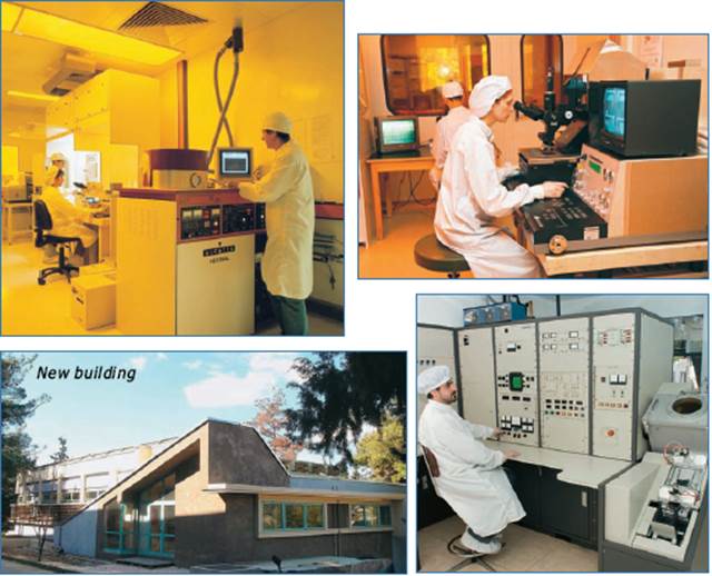
The facilities and equipment of IMEL include a full silicon processing laboratory in a clean room area of 300 m2 equipped with lithography (optical, e- beam) and etching tools, thermal and chemical processing facilities, ion implantation, deposition of metals, dielectrics and poly- nanocrystalline silicon by physical and chemical processes (LPCVD, sputtering, e-gun and thermal evaporation), and process inspection equipment. Satellite laboratories include electrical and optical characterization, micromachining and packaging laboratory, resist development laboratory, electron microscopy (SEM, STM/AFM), sensor characterization and testing equipment.
The clean room area for thermal, chemical and reactive ion etching processes of the Institute has been fully upgraded to class 1000, while lithography area to class 100, in the year 2002.
A new building of the Institute has been constructed in 2006 to host the electrical, optical and structural characterization laboratories. A photograph of the building in the final stage of construction is shown in the figure below.
• Management
The Department of Microelectronics (former Institute of Microelectronics –IMEL) is one of the three departments of the Institute of Advanced Materials, Physicochemical Processes, Microsystems and Nanotechnology (IAMPPMN) of NCSR “DEMOKRITOS” that resulted after a governmental decision for merging in 2012. IMEL (Institute of Microelectronics) has been established in the year 1986 as one of the eight Research Institutes of NCSR Demokritos (National Center for Scientific Research), a medium size, multidisciplinary Research Center under the General Secretarial for Re search and Technology of the Ministry of Development.
Due to the large size of the Institute, management is assisted by 3 Department Coordinators elected by the Researchers.
A scientist is in charge of the processing laboratory, which is a central facility used by all scientific groups. There are also programme representatives for the 3 main R&D programmes as they appear on the organizational structure of the Institute.
• Personnel
The personnel of IMEL includes 17 key researchers and several post-doctoral scientists and PhD students. It also includes a group of technicians that operate the central fabrication facility.
Address |
Institute of Microelectronics
NCSR "Demokritos"
Terma (End) Patriarhou Gregoriou Street,
PO Box 60228
Aghia Paraskevi, Athens, GREECE 15310 |
Tel. |
(+30) 210650-3223 |
Fax |
(+30) 210651-1723 |
Website |
http://imel.demokritos.gr/ |
Department Coordinator |
Name |
N.Glezos |
Email |
glezos@imel.demokritos.gr |
Tel. |
(+30) 2106503236 |
Secretary Name |
Name |
M.Karbadaki |
Email |
mkarmp@imel.demokritos.gr |
Tel. |
(+30) 2106503223 |