| |
|
| |
|
| |
|
| |
|
| |
|
| |
Research |
| |
|
| |
|
| |
|
| |
Publications |
| |
|
| |
|
| |
People |
| |
|
| |
|
| |
|
| |
|
| |
|
| |
|
| |
|
| |
|
|
 |
| |
|
| |
|
|
|
| |
|
| |
|
|
|
|
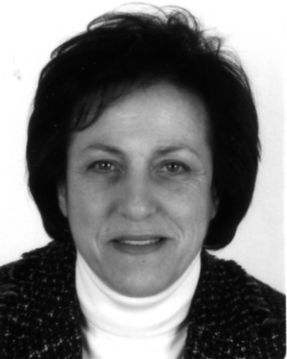
Dr
Androula Nassiopoulou
Director of Research
|
 |
|
Contact
Information
Dr Androula Nassiopoulou
Director of Research , IMEL/NCSR Demokritos
Head of the Nanostructures for Nanoelectronics, Photonics and Sensors (Nano4NPS) Research group
Terma Patriarchou Grigoriou, Aghia Paraskevi
153 10 Athens, Greece
Tel. 0030 210 650 3411
FAX. 30 210 65 11 723
Email:
|
Androula Nassiopoulou received the B.Sc. in Physics from the University of Athens in 1975 and the M.Sc. and Ph.D from the University of Paris XI (ORSAY) in 1977 and 1980 respectively. She then moved to the University of Reims, France as Associate Professor, from where she received the “habilitation to direct research” (Doctorat d’Etat) in 1985. She is with NCSR Demokritos, Institute of Microelectronics (IMEL) since 1986, directed IMEL and was member of the board of Management of NCSR Demokritos in 1996-2009 and Vice President of NCSR Demokritos in 2001-2003. She is currently a “Director of Research” at NCSR Demokritos (IMEL), Head of the “Nanostructures for Nanoelectronics and Sensors” research group, member of the Scientific Community Council of the EU Nanoelectronics platform (ENIAC), member of the Governing Board of the European Institute of Nanoelectronics (Sinano) and President of the Greek National Scientific Society “Micro & Nano”. Her current research interests are on Si nanostructures and nanostructured porous materials for applications in RF, sensors, solar cells and nanoelectronic devices. She is author/co-author of more than 250 publications in international journals and reviews, chaired or co-chaired more than 15 international conferences, edited/co-edited 15 research paper volumes (special issues in specific research fields and conference proceedings) and supervised more than 20 PhD theses.
EDUCATION
- BSc in Physics, University of Athens 1975
(Performance: 1972 entrance examination grade 2nd among all Cypriots, scholarship for all 4 years of the University)
- MSc (DEA) in “Electronic Materials and Structures”, Scholarship from the
“Leventis” foundation, University of Paris XI, Orsay, France 1977
- PhD, University of Paris XI, Orsay, France 1980
- Doctorat d’ Etat Es Sciences Physiques, University of Reims, France, 1985
PROFESSIONAL EXPERIENCE
1997-july 2009:
- Director of the Institute of Microelectronics at NCSR “Demokritos”
(Elected by International Scientific Committee in 1997 for a mandate of 5 years,
re-elected for a second mandate in 2001)
- Member of the Board of Management of NCSR Demokritos (1997-2009)
- Vice-President of NCSR Demokritos in 2001-2002
- President of the Board of Research of NCSR Demokritos in 2000-2001
- Member of the Committee of the Technology Park of NCSR Demokritos in 2001-2003, Contribution to the elaboration of the statute of legislations of
NCSR Demokritos for IP and commercialization of research products
- Member of the National Council for Research and Technology (ESET) (2001-
2002)
- Member of the Scientific Advisory Group of NMP-FP6 (Research Priority:
“Nanotechnology, Materials and Production Processes”, 6th Framework
Programme for Research and Technology in Europe) (2003-2005)
- Member of the Scientific Community Council of AENEAS-ENIAC (European
Technology Platform for Nanoelectronics) (2007-today)
- Founder and currently President of the Board of the Scientific Society
“Micro&Nano” (established in 2004 as a National Scientific Society, counting
today as members five organizations and more than 100 scientists)
- Head of a Research activity on Nanostructures for Nanoelectronics, Photonics
and Sensors”
1988-1997:
- Senior Researcher at IMEL/NCSR Demokritos (1988-97)
- Head of the research activity on “Semiconductor nanostructures science and
applications” (1988-97)
- Head of the Educational Activities of IMEL (1988-96)
1986-88:
- Senior Researcher at IMS/NCSR Demokritos (1986-88)
1980-86:
- Associate Professor at the University of Reims-France, member of the research group on “Surface Spectroscopies and Microscopies”, teaching in the field of
electronics and electron devices (1980-86)
1977-80:
- Research associate (CNRS), University of Paris XI (1977-80)
RESEARCH EXPERIENCE
- Nanostructures /Nanoelectronic devices
Silicon quantum wires and dots, Si/SiO2 superlattices (free standing silicon
nanowires, quantum wires in dielectric), optical and transport properties, light
emitting devices, silicon nanocrystal non-volatile memories, self-assembly,
ordering of nanostructures, alumina templates on silicon for nanostructuring,
nanoparticles in solution
- Porous Si
Mesoporous, macroporous, microporous, porous membranes ever cavity,
applications in electronics (on-chip RF integration porous Si microplates for
local RF substrate isolation), sensors (thermal sensors, microfluidics) and
photonics (2-D photonic crystals)
- Microhotplate technology for thermal sensors
- Porous anodic alumina thin films on Si
Material development, applications as masking material and as template for
nanostructure growth on Si, photonic crystal applications
- Silicon Sensors and Microsystems (MEMs)
Gas flow sensors, gas sensors, acceleration sensors, silicon integrated
thermopiles, silicon micromachining, porous silicon technology for MEMS
fabrication
- Electron Microscopy and Surface Spectroscopies (Auger, XPS, EELS, SEELS,
X-ray Microanalysis, Scanning Electron Microscopy)
|
. |
|
back
to top  |
|