|
|
Equipment The group of micro and nano fabrication using lithography and plasma etching uses the clean room of IMEL for lithographic processes and RIE etching of CMOS compatible materials. The group runs in addition two satellite laboratories: 1. A plasma etching laboratory for non-CMOS processes 1. The plasma etching laboratory
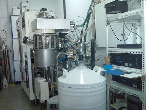
A view of the plasma etching laboratory is shown
above. One can see the plasma etching system (micromachining etching
system) by Alcatel – Adixen. The system is equipped with a high
density helicon antenna plasma source, a magnetically confined diffusion
chamber, a loadlock and a liquid Nitrogen cooling system permitting
operation from -180 C to + 150 C.
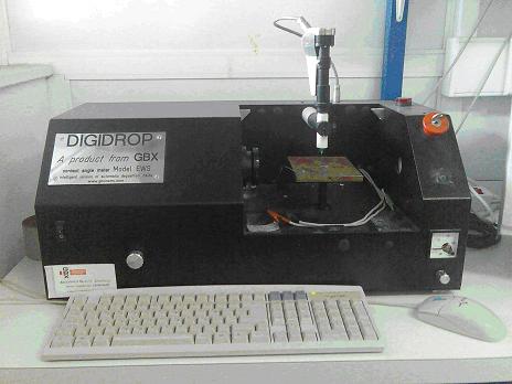
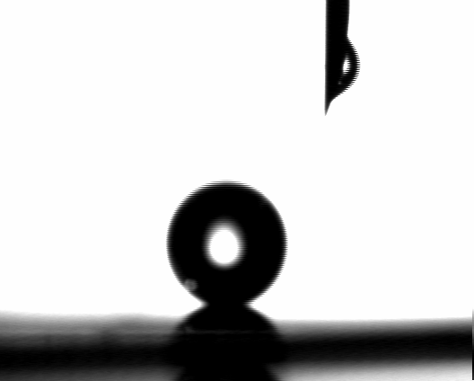
Surface wetting properties are monitored using a contact angle measurement system by GBX Company (see above).
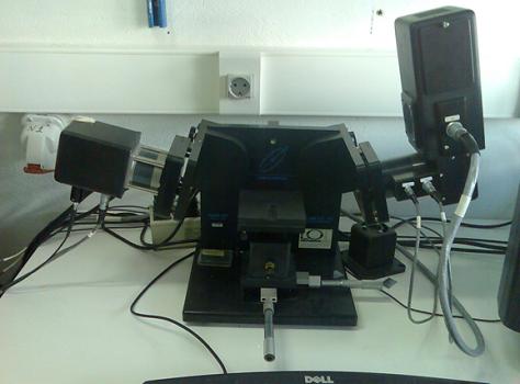
The M2000-F Spectroscopic Ellipsometer system by J.A.WOOLLAM company (see above) may also be used ex-site for film characterization, and is equipped with a heating stage (home made) for thermal property measurements of polymer films (Glass transition temperatures, etc in collaboration with Dr Ioannis Raptis team).
2. Micro-nano fluidics “back end” fabrication and testing laboratory. (under construction)
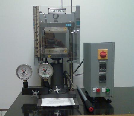
Bonding of plastic microfluidic chips is done using Bonding pressure system by CARVER (see above), which is capable of delivering 12 ton force and a temperature up to 340 C.
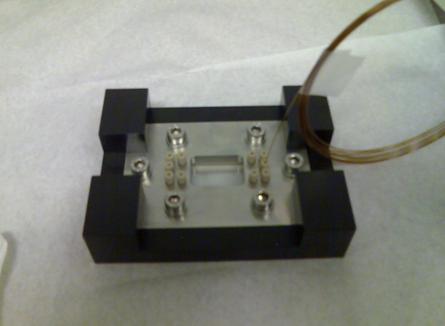
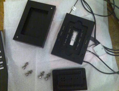
Testing of polymeric or other material based microfluidic devices using a Micronit Lab on Chip Kit.
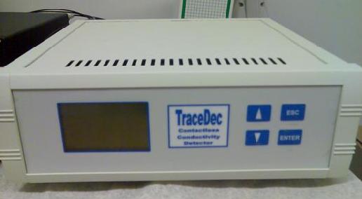
Testing of electrokinetic properties is done using either a home made kit or the electrophoresis kit by Micronit, shown above. Detection is done either using a fluorescence microscope in a nearby laboratory or a contactless conductivity detector by TRACE shown below.
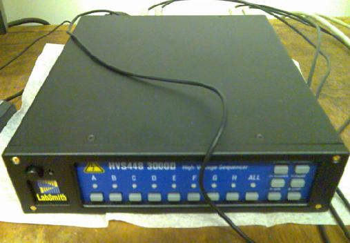
A high voltage power supply by Labsmith is used, see below.
|
|