|
|
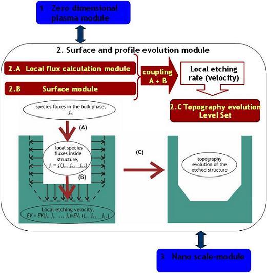
Plasma process simulation • Motivation: One of the greatest challenges in nanotechnology is to find reliable and efficient tools for patterning surfaces on nanometer scale. Plasma etching / processing has been for years one of the basic tools for patterning on micrometer scale. Can it be extended on nanoscale and resolve the above challenge in nanotechnology? Can a plasma reactor be a reliable and efficient tool for nanopatterning in a deterministic or even stochastic way? • Aim: The development of a total multiscale simulator of the processes in a plasma reactor linking the final surface morphology on nanometer scale (roughness, nanotexture or regular patterns) to the input parameters (pressure, power, bias voltage, etc.) which are tuned by pressing the appropriate “buttons” on reactor. Such a simulator could also give hints for plasma process control. This aim can be achieved by dividing the whole
process in a plasma reactor in modules and developing simulation
tools for each module.
1. Zero (or higher) dimensional
plasma module simulating the reactions and kinetics in plasma gas
phase.
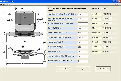
1.
Zero dimensional plasma module Figure 1: The window opened during the run of the zero dimensional plasma module. It contains a diagram of the reactor, the input parameters and the results of the simulation.
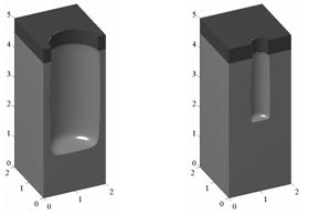
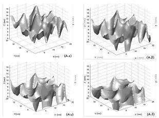
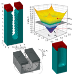
2. Surface Kinetics and profile evolution module: Applications of the level set framework coupled with Langmuir-type surface models. Figure 2a: RIE lag in SiO2 holes etched by fluorocarbon plasma. (Journal of Applied Physics 88 (10), pp. 5570-5584, 2000, Journal of Applied Physics 91 (4), pp. 2697-2707, 2002).
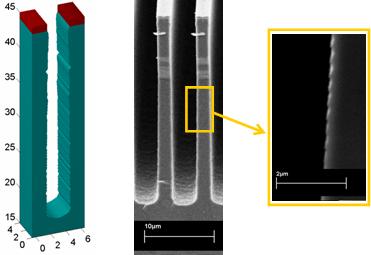
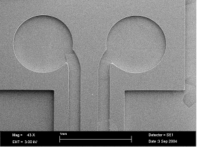
Figure 2b: Simulated and experimental Si trench after etching by the BOSCH process. (to be submitted in 2008).
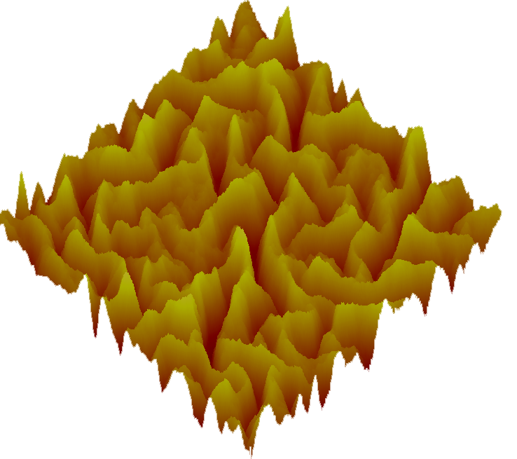
Figure 2c: Wet etching of an initially fractal rough surface. Pushing the continuum approach to the nanoscale (Dynamics Days 2006, to be submitted in 2008).
3. Module
for nanoscale roughness formation: Simulation of nanoroughness formation
during etching of homogeneous or nanocomposite materials using kinetic
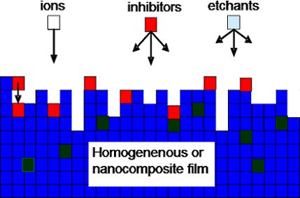
Monte Carlo techniques. Figure 3a: A schematic diagram of the stochastic plasma simulator: 2-D cellular representation of the etched topography and the impinging particles (ions, neutral etchants and etch inhibitors) in the MC simulator for surface etching.
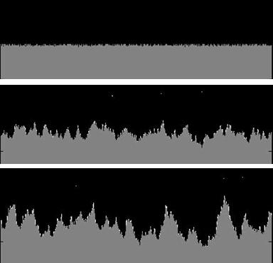
Figure 3b: Application to the etching of homogeneous (Si) films : 2-D snapshots of a Si surface etched by SF6 plasma including the deposition of etch inhibitors (ISNM2005, AVS 2006, 2007, PESM 2007, Phys. Rev. B 2007)
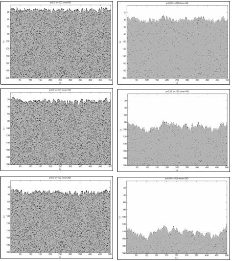
Figure 3c: Application to the etching of nanocomposite materials : 2-D snapshots of the surface morphology of two nanocomposite films with different concentrations of etch resistant filler (10% for the film in the left column of snapshots and 1% for the film in the right column). (Dynamics Days 2006, IEEE, Transactions on Plasma Science 35, p.1359 (2007)).
|
|