 |
|
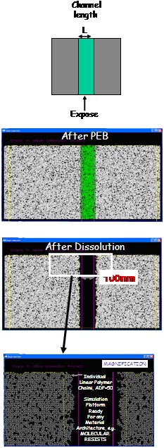
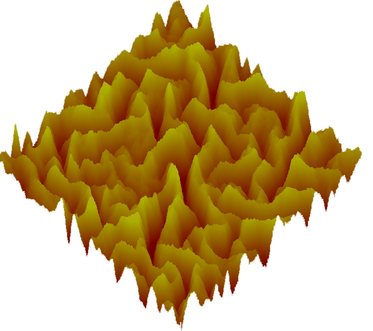
Micro-nano lithography • Our aim : To understand the lithographic behaviour of materials at the nanoscale. To find the material / process origins of Line Edge/Width Roughness (LER or LWR) and propose solutions for its reduction. This can be achieved by means of: 1. Stochastic Simulation of lithography for LER reduction We have developed a 2D and 3D lithography simulator, which inputs individual photoresist molecules / chains, photoacid generator molecules and performs all lithography steps (exposure, PEB, reaction-diffusion, development).
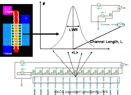
2. Modeling of LER impact on transistor performance
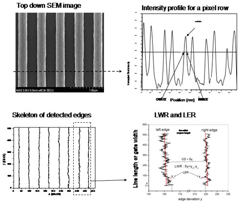
“Slicing” the gate in order to take into accound LWR we can then apply SPICE like electrical analysis and determine quantities such as threshold voltage shift or leakage current variations in terms of LWR. 3. Metrology and characterization of LER/LWR Metrology : LER/LWR extraction from top-down SEM images.
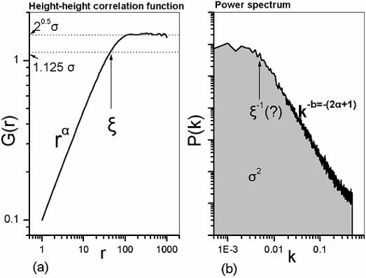
Characterization : a three parameter model.
a) σLWR(inf): the sigma value of the infinite line
length. b) Correlation length ξ : The line length after which line widths
are c) Roughness exponent a: A demo of our software is available on our web page, see under
software. |
|
