|
Project Information per year
2012 - 2011 - 2010 - 2009 - 2008 - 2007 - 2006 - 2005 - 2004
PROJECT I.2
Plasma Enabled Nanofabrication: Processing, Simulation, Metrology and Applications
Key researchers: E. Gogolides, A. Tserepi
Permanent Scientific Staff: V. Constantoudis
Post Doctoral Scientists: G. Kokkoris, D. Moschou, N. Vourdas, K. Tsougeni, G. Papadakis
Collaborating researchers:
- For activity A-Plasma Nanofabrication: I. Raptis (optical characterization), A. Olziersky (e-beam lithography)
- For activity D2-Microfluidics-Lab on Chip for Life Sciences: S. Chatzandroulis, K. Misiakos
- For activity D3-Nanodevices for Energy: P. Argitis, P. Normand, P. Dimitrakis, M. Vasilopoulou
PhD Students: M.-E.Vlachopoulou, A. Malainou, D. Kontziampasis, K. Ellinas, A. Smyrnakis, N. Skoro, V.K. Murugesan Kuppuswamy
MSc Students: A. Zeniou, E. Kouris, N. Karasmani, S. Mouchtouris, Th. Christoforidis
External collaborators:
- For activity A-Plasma Nanofabrication: C. Cardinaud (Univ. of Nantes, France), W. Coene, M. Riepen, M. Van Kampen (ASML, Netherlands), D. Ehm (Zeiss, Germany), U. Cvelbar (Josef Stefan Inst., Slovenia), N. Puač, S. Lazovic (Inst. of Physics, Belgrade, Serbia)
- For activity B-Nanometrology: W. Coene (ASML, Netherlands), G. Gallatin (NIST, USA), R. Gronheid, A.P. Vaglio (IMEC, Belgium), E. Pargon (CEA/LETI, France)
- For activity C-Modeling and Simulation: A. Boudouvis, N. Cheimarios, G. Pashos, (NTUA, Greece), C. Vahlas (U.de Toulouse, France), P. Brault, A.L. Thomann (Univ. d’Orléans, France), G. Gallatin (NIST, USA)
- For activity D1-Smart Nanostructured Surfaces: A. Boudouvis, A. Papathanasiou, D.P. Papageorgiou, C. Charitides, E. Pavlatou (NTUA, Greece), K. Beltsios, I. Panagiotopoulos (Univ. of Ioannina, Greece), E. Amanatides, D. Mataras (Univ. of Patras, Greece), H. Zuilhof, S. Pujari (Wageningen Univ., Netherlands)
- For activity D2-Microfluidics-Lab on Chip for Life Sciences: S. Kakabakos, P. Petrou (IRRP, NCSR-D, Greece), A. Vlahou, S. Pagakis (IIBEAA, Greece), G. Kaltsas (TEI of Athens, Greece), D.S. Mathioulakis (NTUA, Greece), E. Sarantopoulou (NHRF, Greece), E. Gizeli (FORTH, Greece), A. Speliotis (IMS, NCSR-D, Greece), T. Rudin, S.E. Pratsinis (ETH Zurich, Switzerland), J.L. Viovy, S. Descroix (Inst. Curie, France), B. Depuis (Inst. Pasteur, Paris, France), G. Jobst (Jobst Technologies, Germany)
- For activity D3-Nanodevices for Energy: S. Christiensen (IMPP, Germany)
OBJECTIVES
The activities of project I.2 can be seen schematically below:
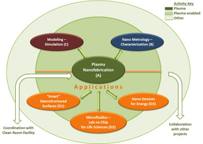
Fig.1. Schematic of project I.2 activities for Plasma Enabled Nanofabrication
The heart of our activities and our first objective is to advance and promote plasma nanofabrication, nanopatterning and plasma nanotechnology enabling various applications. This is seen as the central circle in Fig.1 and described in section A below.
Around plasma nanotechnology a series of activities for nanometrology-characterization (B), modeling-simulation (C) and applications (D) are clustered depicted visually in the second circle around A. A third outer circle includes other activities not directly enabled by plasma nanotechnology but linked to the activities of the second circle (B, C, D), as well as to other projects.
Indeed, after fabrication of micro and nanostructures and devices using plasma processing, our second objective is to develop nanometrology and characterization methodologies for nanostructure description (see section B). Our third objective is to understand and improve plasma and other processes using modeling and simulation (see section C). Finally, our fourth objective is to exploit our plasma nanotechnology toolbox to enable a variety of applications including Surface Engineering (“smart surfaces” see section D1), Microfluidics and Lab on Chip for Life Sciences (see section D2), and NanoDevices for Energy (see section D3). For all these objectives, we work in coordination with the clean room facility, often transferring samples to and from it, and in collaboration with several other projects such as the Biomicrosystems project, and the Lithography project.
For 2012 our main achievements are:
Plasma Nanonofabrication: We improved our new planar technology to fabricate, nanotexture (nanoroughen) and surface-modify polymeric microfluidics and bioMEMS (cf. A.1). We established our recent plasma-directed assembly process for nanodot formation on plasma etched polymers (cf. A.2). We characterized Hydrogen Plasmas for plasma cleaning of sensitive optical surfaces (cf. A.3). We developed two novel plasma processes for ultra high aspect ratio fabrication of Silicon Nanowires and nanopillars and measured their optical properties (cf. A.4).
Nanometrology: We developed a methodology to measure the thickness of thin protein and other films on nanostructured surfaces using AFM data (cf. B.1). We developed software for the extraction of noise from SEM images and measurement of Line-Edge-Roughness (cf. B.2). We initiated the use of complex network theory for the description of rough surfaces (cf. B.3).
Modeling and Simulation: We proposed a simple model and rules of thumb for Line-Edge-Roughness Transfer during Plasma Etching (cf. C.1). We modeled Hydrogen Plasmas for Surface Cleaning (cf. C.2). We modeled the lithography process effects on Contact-Edge-Roughness (cf. C.3). We performed Multiscale and molecular Dynamics Simulations for Chemical Vapour Deposition of Si and Al (cf. C.4, C.5). We developed a computational framework for calculation of Cassie-Wenzel transition of drops sitting on microstructured surfaces (cf. C.6).
“Smart” Nanostructured Surfaces: We developed hierarchical superoleophobic surfaces on organic polymers (PMMA, PEEK, PS, PET etc) and on silicones (PDMS) using Oxygen and SF6 plasma nanotexturing, respectively. New self-assembled fluorinated monolayers were used for their surface energy reduction. Low hysteresis and high contact angle were obtained for several oils (cf. D1.1, D1.2, D1.3).
Microfluidics and Lab on Chip for Life Sciences: We compared the flow in rough hydrophilic and superhydrophobic microchannels using pressure drop and Particle Image Velocimetry experiments, and showed the reduced pressure drop and large slip velocities in the second case (cf. D2.1, D2.2). We fabricated TiO2 affinity microcolumns and demonstrated phosphopeptide enrichment (cf. D2.3). We fabricated a DNA amplification Lab on Chip (μPCR) on a polymeric substrate with accurate temperature control (cf. D2.4). We developed new nanoscale arrays of proteins using colloidal lithography followed by plasma etching and selective protein immobilization (cf. D2.5).
Nanodevices for Energy: We established our first Silicon Nanowire p-n junction devices and demon
FUNDING
- SPAM, Marie Curie-ITN,Contract No 215723
- “DNA on waves: an integrated diagnostic system” GSRT Contract No. LS7(276)
- CORSED, Contract No. PE8(844)
- Love Food, Contract No. 317742
- Plasma Nanofactory, Contract No. 695
- DesireDrop, Contract No. MIS 380835
- Project III41011 of MESTD of Serbia and Post Doctoral Fellowship from Serbian Government for Dr Nevena Puac
|